USING
POWER MOSFETs to Drive Resonant Transformers
Gary L. Johnson,
Ph.D.
Introduction
The most
common way of supplying power to a Tesla coil or resonant transformer is
through a spark gap. A fixed gap is used for smaller sizes, while a
rotating mechanical commutator is used with the
larger sizes. These certainly do their job, but have some
disadvantages. One is the sparking during operation. Any electrical
discharge will dissipate energy in the form of heat, light, and chemical
energy. The breakdown voltage and the amount of energy transferred are
difficult to maintain at constant values as atmospheric conditions change and
as the stationary gap or commutator becomes worn or
dirty. Another disadvantage is that gaps require operation at nearly full
power, even while a new system is being tested and tuned.
Vacuum tube
drivers have been used in the past for small systems. Today, power MOSFETs can be used to drive small demonstration units or
to help tune the larger units before they are operated at full power.
This paper is an introduction to the topic.
MOSFET
Theory
Power MOSFETs (Metal Oxide Semiconductor Field Effect Transistor)
are widely used in switching power supplies. The symbol for an N channel
device is shown in Figure 1. When no voltage is applied between the gate G and
the source S, there will be no path or channel between the drain D and the
source. The device acts like an open switch. When the gate is made
several volts positive with respect to the source, a channel is produced and
current can flow from D to S. The diode in the symbol is produced by the
manufacturing process for power MOSFETs but not for
small signal MOSFETs). Therefore the power MOSFET is basically a high speed switch in parallel with a
diode. The diode has the characteristics of a fast recovery diode.
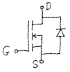
Figure 1. N
channel device symbol.
Power Ratings
A wide
variety of power MOSFETs are commercially
available. The IRF82O, for example, is rated at 500V, 2.5A continuous or
10A pulse, and a resistance of 3 ohms between drain and source when on. The
cost is slightly over a dollar in small quantities. The IRF640 is rated at
200V, 18A continuous or 72A pulse, with an on resistance of 0.18 ohms.
The cost is about four times that of the IRF820. It is possible to get
power MOSFETs with rated voltages up to 1000V.
Higher voltages can be obtained by connecting the power MOSFETs
in series.
These power
levels are not trivial. If we operate at 150V and 18A, the power being
supplied is (150)(18) = 2700W. This should drive a
small Tesla coil in a very satisfactory manner.
After
burning up a dozen or so MOSFETs, I learned that the
current ratings listed require very special heat sinking to get even close to
the specification. The power dissipated in the IRF640 at 18A is I2R
= (18)2(0.18) = 58W in a device with about the volume of a 5 W
resistor. A large heat sink is essential. Even with a good heat
sink, I would not suggest exceeding 6 to 8A with the IRF640 unless a good fan
is also available.
A good power
MOSFET shows a very high resistance between any pair
of leads, except when the diode test function of the multimeter
is used between the source and drain. Most failures that I observed had
at least one pair of terminals shorted together.
Electrical Isolation
The logical
place to put the MOSFET in the circuit is between the
high voltage terminal of the supply and the high voltage terminal of the
load. This means that when the MOSFET is
conducting, both S and D are above ground. Therefore the gate circuit
must be operated without any ground connection. One way of obtaining this
isolation is to use optoisolators and a local 9V
battery to supply the gate voltage. The optoisolator
that I selected is the H11L3, which has the circuit shown in Figure 2.
When a few milliamperes of current are supplied to
the light emitting diode (LED) by a function generator or other source of
pulses, the Schmidt trigger output of the optoisolator
drops from logic high to logic low. The electrical isolation between the
LED and the Schmidt trigger is 2500V(rms), more than adequate for most tests. The
equivalent optoisolator made by Motorola has an
isolation of 7500V, so higher values are available if needed.
The optoisolator circuit is shown in Figure 3. The
function generator circuit supplies a pulse train through a coaxial cable and
current limiting resistor R, to the LED. R,
should be selected to allow adequate current to the LED, but without
overloading the function generator. For example, suppose the lowest
voltage expected at the optoisolator end of the cable
is 7V. The LED voltage would not be more than about 1V, so R1
needs to drop about 6V. The specification for the H11L3 is that it will
change state for not more than 5mA of LED current. By measurement, the
highest LED current required for a group of 10 chips was 1.84 mA. Rounding this off to 2 mA
allows us to select R, = 6/2 = 3k ohms. If the source is not current
limited, a value closer to 1k ohm might be better.
Power is
supplied to the Schmidt trigger portion of the optoisolator
and to the gate of the power MOSFET by a 9V battery,
with a switch to conserve battery life when the circuit is not in use.
The 270 ohm resistor is a pullup resistor required by
the Schmidt trigger output. We want a noninverted
output so we connect the gate to +9V rather than connect the source to
-9V. When pin 4 goes low with respect to pin 5,
at the same time it goes high (actually inverted high) with respect to pin
6. This will put nearly 9 V on the gate with respect to the source, more
than enough to fully turn on the power MOSFET.
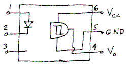
Figure 2 - Schematic of the H11L3 optoisolator IC.

Figure 3 - Circuit utilizing the H11L3 optoisolator IC.
Switching Speeds
This optoisolator is rated for a supply voltage between 3 and
16V, so the 9V battery is well within the operating range. Its maximum
switching speed is 1 MHz in a non return to zero logic system. The
highest speed I have been able to get is about 300 kHz, which is still far
above the switching speed of a mechanical commutator.
With a
different optoisolator, the MOSFET
could supposedly switch at still higher speeds. The sum of the turn-on
delay time, the rise time, the turn-off delay time and the fall time is 230ns
for the IRF640 under specified test conditions. This would yield an
absolute maximum switching speed of 4.35 MHz.
This can be misleading because it is only possible with a
very low function generator impedance, so the gate to source capacitance
can be charged and discharged quickly. With a generator impedance of 50
ohms, rather than the 4.7 ohms specified in the test, the switching time
increases by at least a factor of three [1]. Therefore, if switching
speeds much faster than 300 kHz are required, a different optoisolator
would be required, and possibly a buffer acting as a low output impedance gate
driver.
Using an optoisolator allows the power MOSFET
to be mounted very near the coil under test, but with the function generator
and other test equipment in a shielded environment some distance away.
The Schmidt trigger output will help shape the pulse being input to the gate if
the rise and fall times of the function generator output are not very
fast. The optoisolator and power MOSFET should be shielded in the presence of high electric
and magnetic fields, at least in an aluminum box.
Application Circuit
The basic
circuit for applying pulses to a coil is shown in Figure 4. The diode D, provides a path for current to flow from the inductive
coil when the MOSFET is turned off. It should
be of the fast recovery type [such as FR 304]. At low frequencies, the
coil will appear as an inductor, with the current shown in Figure 5. At
resonance, the output voltage of the coil is nearly sinusoidal, which requires
a sinusoidal input current, as shown in Figure 6. The resistor R, is chosen to force the decay portion of the cycle to be
approximately the same length as the rise portion. This helps the current
to become sinusoidal as resonance is approached. Note that we can have a
sinusoidal current even while applying what is basically a square wave voltage.
Mid-frequency Model
A coil of
wire behaves as an inductor only at low frequencies, well below the operating
frequency of a resonant transformer. At frequencies of interest, it
really needs to be treated as a distributed circuit, or a type of transmission
line [2]. This analysis is not easy, and requires a good background in
electromagnetic theory. A less sophisticated approach which helps explain
some of the phenomena is to consider a lumped model such as Figure 7. The
coil has interwinding capacitances, which are shown
in the figure as a lumped capacitor CL. The diode has stored
charge in the reversed biased mode which must be removed before it can conduct in
the forward direction. This can be represented by CD. At
the instant the MOSFET is switched off, CD
would be charged to the supply voltage VB. CM is
the capacitance between drain and source of the MOSFET.
It would be uncharged at the instant the MOSFET is
turned off.
Figure 4 - Pulse application circuit for
coil.
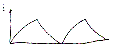
Figure 5 - Current in coil at low
frequencies.
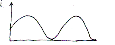
Figure 6 - Current in coil at resonant
frequencies.
At the
instant of MOSFET turnoff, there is a current iL flowing, which
cannot change magnitude instantly because of the inductance. However, it
starts to decrease according to VL = L di/dt. This current is
being supplied by the discharging currents from CD and CL
and the charging current through CM. The inductor and these
three capacitors form a resonant circuit. The voltage across CL
goes to zero while current is still flowing down in the inductor and then
becomes negative as the bottom plate of CL is positively charged by iL. At a later
time, iL will
become zero, and all the initial energy is stored in the capacitors. The
capacitors then start driving current up in the coil in the usual fashion of a
parallel resonant LC circuit.
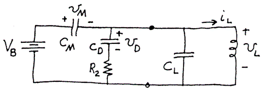
Figure 7 - A lumped component model of a coil
circuit.
Analysis is
complicated by the two diodes in the circuit. As soon as VL goes negative, D1 starts to
conduct, dissipating part of the stored energy in R2 and limiting
the negative voltage swing. If the system still has enough energy stored
for VL to exceed V, on the positive cycle,
then the MOSFET diode will conduct, thereby clamping
the coil voltage at VB.
From this
analysis, it can be seen that the diode D1 is not always essential
to the circuit operation. It acts to limit the negative voltage swing,
which primarily protects the MOSFET from being
operated in reverse breakdown or avalanche mode. Modern MOSFETs are rather rugged and can withstand avalanche
operation if the total energy dissipated is not too large. Also, it is quite
possible that the inter-electrode capacitance can absorb all the initial
magnetic energy without exceeding the MOSFET
breakdown voltage. The energy stored in a capacitor is proportional to
the square of the voltage, so if VB is one tenth of the breakdown
voltage, CL can store one hundred times the energy on the negative
half cycle as it had before the MOSFET was switched
off. One can check this by making R2 larger and looking at the
negative swing of VL on an
oscilloscope. If the MOSFET voltage rating is
not being exceeded with a large R2 then the diode can be removed
entirely.
This leaves
the built in diode of the MOSFET which could be
clamping the positive swing of the coil voltage. If a symmetric swing is
desired, a diode can be placed in series with the MOSFET,
as shown in Figure 8. This circuit forces all the energy supplied to the
coil during the MOSFET on-time to remain in the coil
until dissipated as heat. This is the most efficient circuit and has the
longest oscillatory decay.

Figure 8 - The most efficient coil circuit.
Conclusion
Power MOSFETs are quite suitable for driving small resonant
transformers and Tesla coils at frequencies up to about 200 kHz. They can
also be used in tuning and optimizing larger units at reduced voltage and power
levels. The optimum on-time and cycle time of a mechanical commutator can be determined before the commutator
is built, thus saving either improper operation or wasted effort.
References
[1]
Motorola Power MOSFET Transistor Data Book, 1988.
[2]
Corum, James F. and Kenneth L. Corum,
"A Technical Analysis of the Extra Coil as a Slow Wave Helical
Resonator," Proceedings of the 1986 International Tesla Symposium, pp. 2-1
- 2-24.